


With the European Chips Act aiming to bolster Europe’s standing in the global semiconductor landscape, the NanoIC pilot line stands at the forefront of advancing semiconductor technology. By serving as a vital link between research breakthroughs and practical applications, NanoIC contributes significantly to Europe’s leadership in semiconductor innovation.
To facilitate the transition from research to market in the semiconductor sector, a robust connection between laboratories and fabrication facilities is essential. The NanoIC pilot line focuses on advancing computing system architectures by refining specific semiconductor technologies, with a vision to empower European companies to lead in semiconductor innovation.
The NanoIC pilot line offers a beyond 2nm system-on-chip (SoC) pilot line dedicated to developing and refining advanced logic, memory, and interconnect technologies. Through large-scale capacity building and collaboration in imec’s cleanroom in Leuven, Belgium, the project aims to accelerate the maturation of cutting-edge technologies for prototyping and innovation support, providing the semiconductor ecosystem access to these advancements.
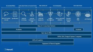
NanoIC Consortium
Imec leads the NanoIC pilot line project consortium, joined by CEA-Leti in France, Fraunhofer-Gesellschaft (FhG) in Germany, VTT Technical Research Center in Finland, Tyndall National Institute in Ireland, and the Center for Surface Science and Nanotechnology of the University Politehnica of Bucharest in Romania. Supported by the Flemish Government, other participating states, and the Chips Joint Undertaking, the consortium collaborates to ensure the successful implementation of the pilot line.
Future Compute Systems
The progression in logic devices, particularly the nanosheet class, is anticipated to drive scaling and performance through upcoming generations. Complementary field effect transistor (CFET) architectures are projected to revolutionize CMOS device design around 2031, emphasizing the need for extensive research in new materials, process modules, and advanced lithography techniques.
Memory innovations focus on novel magnetic memories such as spin orbit torque-magnetic random access memory (SOT-MRAM) and embedded Dynamic Random Access Memory (eDRAM). Developing alternative configurations and exploring new materials are essential to meet the memory capacity and bandwidth demands of future workloads.
Integrating different dies into systems necessitates advanced electrical and optical interconnects beyond 2nm. The NanoIC pilot line focuses on enabling 3D heterogeneous integration through die-to-wafer (D2W) hybrid bonding techniques, facilitating side-by-side die connections and 2.5D chiplet integration on a low-cost interposer platform.
The key logic, memory, and interconnect technologies defined by NanoIC at industry-relevant dimensions form the core of the pilot line’s initiatives. Evaluating new processes and materials, enhancing process control, and establishing validation routes are essential components in enabling these technologies. By investing in new processing and metrology tools, NanoIC aims to pave the way for continuous improvement and innovation collaboration with materials and equipment vendors.
Facilitating Advanced Chip Designs with PDKs
The NanoIC pilot line offers advanced process design kits (PDKs) to European designers in academia and industry, providing comprehensive toolsets for predictive modeling, cell libraries, and system-level integration resources. These PDKs enable designers to simulate and validate integrated circuits accurately, supporting innovation in beyond 2nm nodes and addressing complex design challenges.
Two types of PDKs are available through NanoIC: pathfinding PDKs for early design exploration in advanced IC technologies, and system exploration PDKs for hardware prototyping and system-level innovation. These PDKs cover various logic, memory, and interconnect technologies, allowing designers to explore upcoming chip architectures and support innovation in future nodes.
Throughout the project, NanoIC will release multiple versions of the N2 pathfinding PDK, along with logic and memory PDKs based on eDRAM and SOT-MRAM advancements. Advanced interconnect solutions can be explored through various PDKs, including RDL, silicon interposer, and D2W hybrid bonding.
Driving Innovation in Europe
The NanoIC pilot line offers flexible access to advanced semiconductor technologies for the entire ecosystem, fostering collaboration among companies, research institutes, start-ups, and universities. Integrated device manufacturers, foundries, equipment suppliers, and design companies can leverage the pilot line’s baselines to explore new modules, enhance performance, and refine tools and processes.
In addition to facilitating technological advancements, the NanoIC pilot line is dedicated to nurturing the next generation of semiconductor experts. Through partnerships with EU Competence Centers, NanoIC offers educational courses on beyond 2nm technologies, providing students with real-world experience and industry-oriented training to prepare them for future challenges.
Overall, NanoIC plays a crucial role in bridging the gap between cutting-edge research and practical applications in the semiconductor industry, emphasizing Europe’s commitment to innovation, competitiveness, and sustainable growth in the digital era.
Disclaimer
The NanoIC pilot line’s acquisition and operation are jointly funded by the Chips Joint Undertaking, through the European Union’s Digital Europe (101183266) and Horizon Europe programs (101183277), along with support from participating states. For more information, visit the NanoIC project website.
This article is inspired by a comment published in Nature Reviews Electrical Engineering (Volume 1 | December 2024 | 764–765 | 764).
Kindly note that this article will also feature in the upcoming edition of our quarterly publication.

